| Nanotechnology | |||||||
Zinc oxide nanowires make ultrasensitive photodetectors30 April 2007 The geometry of semiconducting nanowires makes them uniquely suited for light detection, according to a new University of California study that highlights the possibility of nanowire light detectors with single-photon sensitivity.
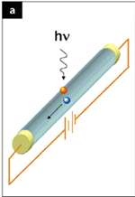
Nanowires are crystalline fibres about one thousandth the width of a human hair, and their inherent properties are expected to enable new photo-detector architectures for sensing, imaging, memory storage, intrachip optical communications and other nanoscale applications, according to a new study in an upcoming issue of the journal Nano Letters. The University of California San Diego (UCSD) engineers illustrate why the large surface areas, small volumes and short lengths of nanowires make them extremely sensitive photodetectors — much more sensitive than larger photodetectors made from the same materials. "These results are encouraging and suggest a bright future for nanowire photodetectors, including single-photon detectors, built from nanowire structures,” said Deli Wang, an electrical and computer engineering (ECE) professor from the UCSD Jacobs School of Engineering and corresponding author on the Nano Letters paper. For a nanowire to serve as a photodetector, photons of light with sufficient energy must hit the nanowire in such a way that electrons are split from their positively charged holes. Electrons must remain free from their holes long enough to zip along the nanowire and generate electric current under an applied electric field — a sure sign that light has been detected.
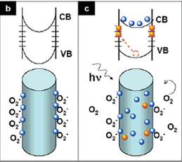
The new research demonstrates that the geometry of nanowires — with so much surface area compared to volume — makes them inherently good at trapping holes. Dangling bonds on vast nanowire surfaces trap holes, and when holes are trapped, the time it takes electrons and holes to recombine increases. Delaying the reunion of an electron and its hole increases the number of times that electron travels down the nanowire, which in turn triggers an increase in current and results in “internal photoconductive gain.” “Different kinds of nanowires detect different wavelengths of light. You could make a red-green-blue photodetector on the nanoscale by combining the right three kinds of nanowires,” said Cesare Soci, one of two primary authors on the Nano Letters paper and a postdoctoral researcher in the Deli Wang lab at the Jacobs School. The other primary author is Arthur Zhang, a graduate student in the lab of Yu-Hwa Lo, an electrical engineering professor at the Jacobs School. This work supports recent theoretical work from Peter Asbeck’s High Speed Device Group, also at the Jacobs School. “Our theoretical work showed that light-induced conductivity in nanowires can be increased by more than 10 times over similar bulk structures under the same illumination level. The work from Deli Wang’s lab has confirmed some of our calculations and provides further support for the idea that nanowires will be increasingly incorporated into photodetection and photovoltaic applications,” said Asbeck. In the new work, short pulses of ultraviolet light (hundreds of femtoseconds wide) were detected on time scales in the nanosecond range. Moreover, using electronic measurement of photocurrent, the engineers reported internal photoconductive gain (G) as high as 108 — one of the highest ever reported. “Although nanowire detectors offer both high speed and high gain, the most important figure of merit for the device is the signal-to-noise ratio or the sensitivity,” explained Yu-Hwa Lo, an author on the Nano Letters paper and the director of NANO3, the clean nanofabrication facility at Calit2's UCSD campus. “Because of the unique geometry of nanowires, the active volume that produces dark current, a source of noise, is only one thousandth that of a normal size photodetector. This enables nanowire detectors to achieve very high sensitivity, provided that light can be efficiently coupled into the nanowires. Several methods have been proposed to achieve light coupling efficiency, such as placing the nanowires in an optical resonant cavity. In theory, a nanowire detector can achieve single photon sensitivity, which is the ultimate sensitivity for any photodetector,” said Lo. The engineers also show that molecular oxygen absorbed at the surface of zinc oxide (ZnO) nanowires capture free electrons present in n-type ZnO nanowires and make them especially good at keeping holes and electrons apart. The oxygen mechanism the authors outline explains much of the enhanced sensitivity reported in ZnO nanowire photodetectors. The engineers fabricated and characterized UV photodetectors made from ZnO nanowires with diameters of 150 to 300 nanometers and lengths ranging from 10 to 15 micrometers. The researchers studied the photoconductivity of zinc oxide nanowires over a broad time range and under both air and vacuum. Analytical studies performed by Peter Asbeck and ECE graduate student Lingquan Wang and published in the proceedings of IEEE-NANO 2006 support the mechanism outlined in the Nano Letters paper. According to Wang, this work also highlights how moving to the nanoscale can sometimes throw intuitions out the window. “The surface trap states that help to make nanowires such sensitive light detectors are the very same surface features that engineers desperately avoid when manufacturing semiconductors for computer transistors, where they hamper performance,” Wang said.
|